Table of Contents
ToggleIntroduction
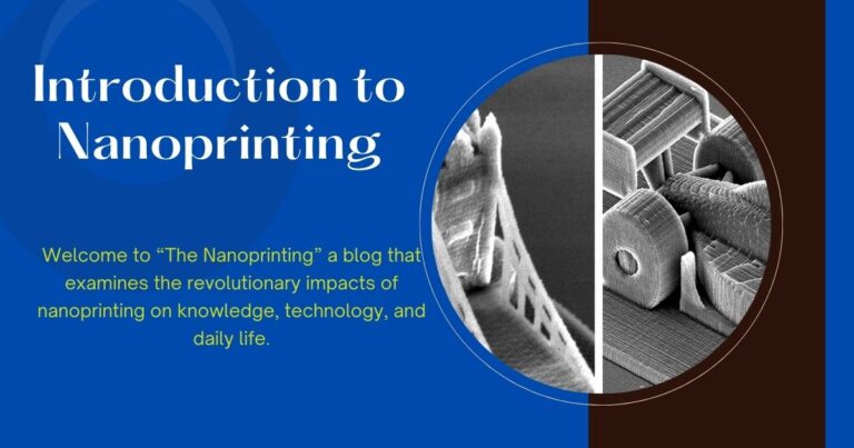
Welcome to “The Nanoprinting,” a blog that examines the revolutionary impacts of nanoprinting on knowledge, technology, and daily life.
We cordially invite you to join us as we investigate the amazing advancements and potential applications of this cutting-edge technology in this microscopic world.
Nanoprinting, a rapidly evolving field that enables the fabrication of complex structures at the nanometer scale, will transform industries like electronics, medicine, and energy.
This technology has ushered in a new era of innovation and established itself as a significant influence on the future by enabling materials to be changed at the atomic level.
We will examine the fundamentals of nanoprinting in this blog, emphasizing its background, scientific foundations, and key innovations. We’ll guide you through the most recent advancements in nanoscale 3D printing, such as brand-new tools, materials, and processes.
Along the way, we’ll also look at the potential drawbacks and moral issues that come with the widespread use of this ground-breaking innovation.
We will discuss real-world applications that are already revolutionizing industries as we navigate the constantly changing nano-printing landscape, including the creation of incredibly efficient solar cells, specialized drug delivery systems, and flexible electronics.
We will also keep you updated on new developments, trends, and research in this fascinating area so you have a complete understanding of the nano-world.
Visit “The Nano Frontier” with us as we set out on an exciting journey into the world of the infinitesimally small, where science fiction becomes science fact and the potential for innovation is truly limitless.
We will explore the wonders of nanoprinting together and experience firsthand how powerful it can be.
What is Nano-Printing?
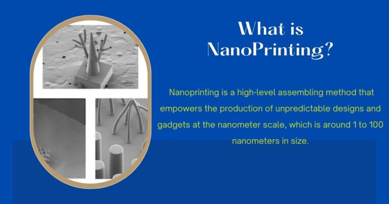
Nanoprinting is a high-level assembling method that empowers the production of unpredictable designs and gadgets at the nanometer scale, which is around 1 to 100 nanometers in size.
A nanometer is one-billionth of a meter, making nano-printing an unbelievably exact and sophisticated technology.
This groundbreaking method can change different ventures, like hardware, medication, energy, and materials science, by allowing the control of materials at the atomic level.
Nanoprinting includes a scope of procedures that are utilized to make nanostructures through cycles like added substance fabricating, subtractive assembling, and self-gathering.
These methods incorporate electron-beam lithography, nanoimprint lithography, dip-pen nanolithography, and two-photon polymerization, among others.
Every method has exceptional benefits and limits, making them appropriate for specific applications and materials.
One of the most widely used methods of nanoprinting called nanoimprint lithography involves pressing and heating a substrate to transfer a pattern from a mold onto it.
Because it produces nanostructures with high resolution, high throughput, and low cost, this method is especially appealing for applications in the semiconductor and electronics industries.
In contrast, dip-pen nanolithography precisely and purposefully deposits molecules onto a surface using an atomic force microscope (AFM) tip as a “pen”.
This technique enables the creation of complex, personalized nanostructures and has been used in industries like biosensing, nanoelectronics, and surface modification.
A laser is used to selectively harden photosensitive materials and build nanostructures layer by layer in yet another noteworthy method for printing nanostructures.
This technique enables the creation of three-dimensional structures with intricate geometries and has shown promise in several domains, including tissue engineering and micro-optics.
The ability to generate materials and gadgets using nanoprinting has the potential to fundamentally alter how we create them.
By utilizing the unique qualities that appear at the nanoscale, such as greater electrical conductivity, increased mechanical strength, and improved biocompatibility, nanoprinting can enable the production of creative solutions to some of the most serious issues confronting the globe.
For instance, ultra-efficient solar cells that can capture more sunlight and produce electricity more effectively were made possible by nanoprinting.
Additionally, nanoprinting has shown considerable promise in the area of medicine, enabling the creation of biomimetic scaffolds for tissue regeneration, enhanced diagnostic tools, and tailored drug delivery systems.
Despite its many benefits, nanoprinting also presents a number of difficulties, including managing the quality and reproducibility of nanostructures as well as resolving issues with the environment and safety related to nanomaterials.
To ensure the secure and long-lasting implementation of this game-changing technology, it is crucial to take these issues into account as we investigate and improve nanoprinting procedures.
A Brief History of Nanoprinting

The invention of scanning probe microscopy (SPM), which allowed researchers to see and work with materials at the nanoscale, is credited with the beginning of nanoprinting.
Gerd Binnig and Heinrich Rohrer created scanning tunneling microscopy (STM), the first SPM method, in 1981. STM made it possible to examine atomic and molecular structures on surfaces.
Midway through the 1990s, Chad Mirkin and his associates created dip-pen nanolithography (DPN), which was the next big advancement in the area.
This method allowed for the controlled deposition of molecules onto a surface using an atomic force microscope (AFM) tip, resulting in nanoscale patterns and shapes.
The discipline of nanoimprint lithography (NIL) also developed at the same time. Using pressure and heat, a design from a mold is transferred onto a substrate using this method.
The viability of NIL for producing structures smaller than 100 nm was established in 1995 by Stephen Chou and his team at Princeton University.
Since then, the method has undergone substantial research and has been tuned for use in a variety of fields, such as microelectronics, optics, and biology.
The advent of two-photon polymerization (2PP) in the early 2000s revolutionized the nanoprinting industry. 2PP creates three-dimensional structures layer by layer by solidifying a photosensitive substance with a focussed laser.
This method enables the high-resolution and precision synthesis of complex, individually designed nanostructures.
Since nanoprinting is still in its infancy, new methods and uses are continually being created.
Recently, researchers have started exploring the possibilities of nanoprinting for creating cutting-edge materials like graphene and carbon nanotubes as well as for use in the sectors of energy, medicine, and environmental cleanup.
Although there have been significant advancements in nanoprinting research since its start, there are still issues with cost, scalability, and reproducibility.
However, because of the quick development of new technologies and materials as well as the expanding need for nanoscale devices and structures, the future of nanoprinting is promising and full of opportunities.
Different Types of Nanoprinting Techniques
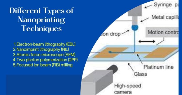
- Electron-beam lithography (EBL):
Electron-beam lithography (EBL) is the process of selectively exposing a resist-coated substrate with an electron beam, producing a pattern that can then be etched into the substrate to produce nanoscale structures. This method is especially helpful for precisely and tightly controlling the creation of high-resolution features.
- Nanoimprint lithography (NIL):
Via pressure and heat, a pattern from a mold is transferred onto a substrate via nanoimprint lithography (NIL). This method is very appealing for applications in the semiconductor and electronics sectors because it can make large-area nanostructures with high throughput and low cost.
- Atomic force microscope (AFM):
An atomic force microscope (AFM) tip is used as a “pen” in dip-pen nanolithography (DPN), which deposits molecules precisely and deliberately onto a surface. This method has been applied in fields including surface modification, nanoelectronics, and biosensing because it enables the development of intricate, specially-made nanostructures.
- Two-photon polymerization (2PP):
2PP is the layer-by-layer construction of three-dimensional structures out of photosensitive materials by the focused laser solidification process. This method has shown promise in a variety of applications, including tissue engineering and micro-optics, and allows for the construction of intricate, specially-made nanostructures with great resolution and accuracy.
- Focused ion beam (FIB) milling:
FIB milling is the process of generating nanoscale features with high resolution and accuracy by selectively removing material from a substrate using a focused ion beam. Applications for this approach include the creation of semiconductor devices and nanoscale imaging.
- Scanning probe lithography (SPL):
Using a probe to manipulate and pattern materials at the nanoscale is known as scanning probe lithography (SPL). SPL techniques include atomic force microscopy (AFM) and scanning tunneling microscopy (STM). These methods are particularly helpful for designing unique nanostructures and researching the atomic-level characteristics of materials.
- Direct laser writing (DLW):
Direct laser writing (DLW) involves selectively modifying a photosensitive material with a focussed laser while layer-by-layer constructing three-dimensional structures. This method has demonstrated promise in a number of applications, including micro-optics and microfluidics, and can produce intricate, specially-made nanostructures with great resolution and precision.
Each nanoprinting method has particular benefits and drawbacks, making it appropriate for certain materials and applications.
For instance, EBL and FIB milling are perfect for producing high-resolution features with a high degree of precision, but NIL and DLW are better suited for producing large-area nanostructures with a high throughput and low cost.
Two-photon polymerization makes it possible to create three-dimensional structures with complex geometries, whereas dip-pen nanolithography and scanning probe lithography are particularly effective for producing custom-designed nanostructures.
New methods and materials will be created as the field of nanoprinting develops, increasing the potential uses and capabilities of this game-changing technology.
Nanomaterials for Nanoprinting
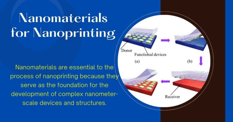
Nanomaterials are essential to the process of nanoprinting because they serve as the foundation for the development of complex nanometer-scale devices and structures.
Nanomaterials are incredibly useful for a variety of applications in industries like electronics, medicine, energy, and materials science thanks to their special qualities like improved electrical conductivity, mechanical strength, and biocompatibility.
The following list includes some of the most popular nanomaterials for nanoprinting:
- Metals: Materials like copper, silver, and gold are frequently used in nanoprinting because of their superior mechanical and electrical conductivity. Transistors and electronic circuits for nanoscale electronic devices are frequently built using these materials.
- Semiconductors: For the manufacture of electronic components, the semiconductor industry heavily relies on semiconducting substances like silicon and gallium arsenide. These materials are ideal for a variety of applications, including photovoltaics, LEDs, and microelectronics, because of their distinctive electronic properties, such as bandgap energy.
- Polymers: Polymers are frequently used in nanoprinting due to their adaptability, low cost, and ease of processing. A wide range of applications, including tissue engineering and drug development, have made use of polymers of all kinds, such as polyethylene glycol (PEG) and polyvinyl alcohol (PVA).
- Carbon-based materials: Due to their distinct electronic, mechanical, and thermal properties, carbon-based materials, such as graphene and carbon nanotubes, have attracted a lot of attention recently. Numerous applications, including high-performance electronics, energy storage, and catalysis, have shown these materials to have great potential.
- Biomolecules: Biomolecules have been used in nanoprinting to make bio-inspired nanostructures and for applications in biosensing and drug delivery. Examples of these molecules include DNA and proteins. These materials excel in a variety of biomedical applications due to their special qualities, including self-assembly and biocompatibility.
Numerous nanomaterials are capable of being used for nanoprinting, depending on the precise application and the desired properties of the final product.
For instance, flexible electronics or biomedical devices can be made of polymers, whereas high-conductivity electronic components can be made of metals.
Biomolecules can be used to create specialized drug delivery systems, while carbon-based materials like graphene and carbon nanotubes can be used to create high-performance energy storage devices.
Important factors to take into account when choosing materials for nanoprinting include material quality and consistency. Any impurities or flaws in the nanomaterials can have a significant impact on the finished product’s properties, which can impact the product’s dependability and performance.
The importance of selecting and describing nanomaterials used in nanoprinting to ensure the desired properties are achieved.
New nanomaterials and material combinations will be created as the field of nanoprinting develops, increasing the capabilities and potential applications of this game-changing technology.
Nanoprinting has a great deal of potential for developing novel solutions to some of the most pressing problems facing humanity.
Nanoprinting in Electronics
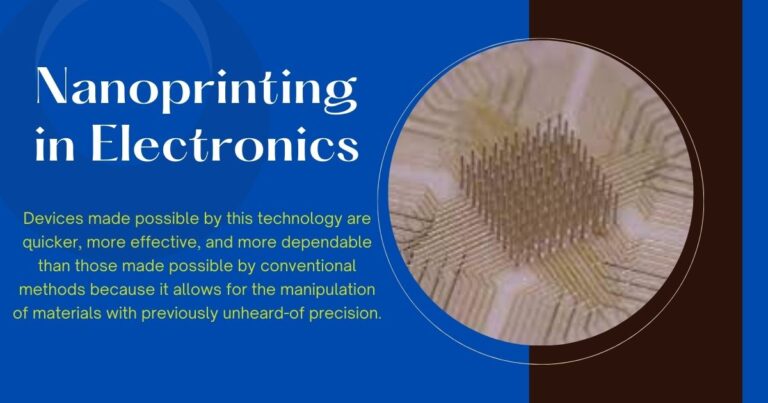
Electronics has a lot of potential for nanoprinting because it can make sophisticated nanometer-scale electronic parts and devices.
Devices made possible by this technology are quicker, more effective, and more dependable than those made possible by conventional methods because it allows for the manipulation of materials with previously unheard-of precision. The following are some applications for nanoprinting in electronics:
- Nanoscale transistors are being created using nanoprinting methods like electron-beam lithography and nanoimprint lithography. These transistors have features smaller than 10 nm. These incredibly tiny transistors are better suited for use in mobile devices and high-performance computing because they switch more quickly and use less power than conventional transistors.
- Flexible circuits: On a variety of substrates, including polymers and paper, flexible circuits can be produced using nanoprinting techniques like direct laser writing and dip-pen nanolithography. These flexible circuits are suitable for use in biomedical devices, smart packaging, and wearable electronics because they are lightweight, inexpensive, and conformable.
- High-density data storage: Magnetic and optical disks, as well as other high-density data storage devices, can be made using nanoprinting techniques, such as focused ion beam milling and nanoimprint lithography, with feature sizes as small as 10 nm. Compared to traditional data storage devices, these have a larger storage capacity and faster access times.
- Sensors: Sensitive and selective sensors can be created using nanoprinting techniques like dip-pen nanolithography and scanning probe lithography. Numerous applications, such as environmental monitoring, medical diagnosis, and food safety, can make use of these sensors.
- Electronic component 3D printing: Complex geometric electronic components, such as micro-optics and microfluidics, can be printed using nanoprinting techniques like two-photon polymerization. High-resolution and precision custom-designed components can be produced using this technology.
- Transparent conductive films: Transparent conductive films can be produced using nanoprinting methods like nanoimprint lithography and electron-beam lithography. These films are used in a variety of products, including touchscreens, solar panels, and LED lighting. These films are perfect for use in optoelectronic devices because they have high conductivity and transparency.
Higher performance, lower power consumption, and smaller device sizes are just a few benefits of using nanoprinting in electronics.
Additionally, nanoprinting enables the production of specially designed components with exceptional precision and accuracy, enabling the creation of creative solutions to challenging issues.
However, the widespread use of nanoprinting in electronics also brings with it difficulties, including the need for scalable manufacturing procedures, affordable materials, and trustworthy quality control.
With more study and development, nanoprinting could completely alter the electronics sector by making it possible to produce components and devices that are quicker, smaller, and more effective than ever.
Nanoprinting in Energy
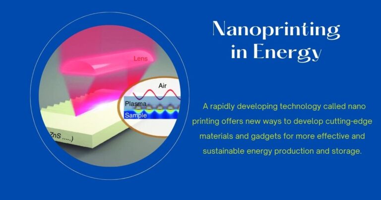
A rapidly developing technology called nanoprinting offers new ways to develop cutting-edge materials and gadgets for more effective and sustainable energy production and storage. The following are some examples of how nanoprinting is used in the energy sector:
- Solar cells: Using nanoprinting methods like two-photon polymerization and electron-beam lithography, highly effective solar cells with improved light absorption and conversion efficiency can be produced. Furthermore, nanoprinting enables the development of specially designed solar cell architectures, like nanowire arrays and plasmonic structures, which can improve the performance of the cells.
- Batteries: Electrodes and separators for micro- and nanoscale batteries can be made using nanoprinting techniques like direct laser writing and nanoimprint lithography. High-capacity, high-performance batteries with quicker charging and longer lifetimes can be made using these components.
- Fuel cells: High-performance fuel cell components, such as catalysts and electrodes, can be produced using nanoprinting techniques like focused ion beam milling and dip-pen nanolithography. These elements make it possible to develop fuel cells for energy production that are more dependable and efficient.
- Energy storage materials: Complex nanostructures and architectures for energy storage materials, such as supercapacitors and metal-organic frameworks, can be produced using nanoprinting techniques like direct laser writing and two-photon polymerization. These materials are ideal for energy storage applications because they have higher energy densities and charge-discharge rates than standard materials.
- Energy harvesting: Energy harvesting devices like piezoelectric and thermoelectric generators can be made using nanoprinting techniques like dip-pen nanolithography and scanning probe lithography. These machines can transform thermal and mechanical energy into electrical energy, offering a dependable and sustainable source of power for a variety of uses.
Higher efficiency, longer lifetimes, and lower costs are just a few of the notable benefits of applying nanoprinting to the energy sector.
Additionally, nanoprinting makes it possible to produce components and materials with a high degree of accuracy and precision that are specifically designed for them, opening the door for the creation of creative answers to difficult energy-related problems.
The widespread use of nanoprinting in energy does, however, bring about a number of difficulties, including the need for scalable manufacturing processes, reasonably priced materials, and trustworthy quality control.
However, nanoprinting has the potential to revolutionize the energy sector through the development of more effective and sustainable energy production and storage technologies. This is provided that research and development efforts are not abandoned.
Nanoprinting in Medicine

Nanoprinting holds great promise for new approaches to create cutting-edge tools and materials for better, more individualized healthcare.
By enabling the manipulation of materials with previously unheard-of precision, this technology produces devices and therapies that are quicker, more effective, and more precisely targeted than their conventional counterparts. Some applications of nanoprinting in medicine include the following:
- Drug delivery: High-precision and accurate custom drug delivery systems can be made using nanoprinting techniques like dip-pen nanolithography and two-photon polymerization. These systems can be configured to release medications at predetermined intervals and locations throughout the body, enhancing their effectiveness and minimizing their side effects.
- Tissue engineering: For tissue engineering applications, such as scaffolds for cell growth and organ-on-a-chip gadgets, complex three-dimensional structures can be produced using nanoprinting techniques like two-photon polymerization and direct laser writing. These structures allow for precise control of cell behavior and the development of useful tissue substitutes.
- Diagnostics: High-sensitivity biosensors for diagnostic applications can be made using nanoprinting methods like scanning probe lithography and nanoimprint lithography. With the help of these sensors, doctors can quickly and accurately diagnose patients’ illnesses, allowing for earlier intervention and better treatment results.
- Implants: Custom-designed implants with exact geometries and surface properties can be made using nanoprinting techniques like focused ion beam milling and electron beam lithography. These implants have the potential to enhance patient outcomes while lowering the danger of complications like infection and rejection.
- Nanoparticles: Nanoprinting methods like dip-pen nanolithography and direct laser writing can be used to produce nanoparticles with precise sizes, shapes, and surface characteristics. Numerous uses for these nanoparticles exist, such as targeted drug delivery, imaging, and sensing.
With higher efficacy, fewer side effects, and more individualized treatment options, nanoprinting in medicine has many benefits.
Furthermore, nanoprinting enables the development of innovative solutions to challenging medical issues by allowing for the high precision and accuracy production of specially designed devices and therapies.
The widespread use of nanoprinting in medicine does, however, come with some drawbacks, including the need for scalable manufacturing processes, reasonably priced materials, and trustworthy quality control.
Furthermore, it is crucial to carefully assess and keep track of the legal and safety aspects of nano-printed medical devices and treatments.
However, by enabling the creation of more effective and customized healthcare solutions, nanoprinting has the potential to revolutionize the medical industry. This is true as long as research and development efforts are continued.
Nanoprinting in Environmental Remediation
The field of environmental remediation is one where nanoprinting has a lot of potentials because it opens up new avenues for developing cutting-edge products and materials that will make cleaning up contaminated sites more effective and sustainable.
By enabling the manipulation of materials with previously unheard-of precision, this technology produces devices and materials that are quicker, more effective, and more targeted than their conventional counterparts. The following are some applications for environmental remediation using nanoprinting:
- Water purification: Highly accurate and precise water filtration systems can be made using nanoprinting techniques like two-photon polymerization and direct laser writing. Heavy metals, organic pollutants, and microorganisms can all be eliminated from water using these systems.
- Soil remediation: Custom-designed nanomaterials can be made for soil remediation using nanoprinting techniques like focused ion beam milling and electron beam lithography. Heavy metals, organic pollutants, and pesticides can all be eliminated from soil using these materials at the nanoscale.
- Air purification: High-sensitivity biosensors for air pollution monitoring can be made using nanoprinting techniques like dip-pen nanolithography and scanning probe lithography. Nitrogen oxides, volatile organic compounds, and particulate matter are just a few of the air pollutants that these sensors can identify and measure.
- Nanocatalysts: For use in environmental remediation applications, custom nanocatalysts can be made using nanoprinting techniques like two-photon polymerization and direct laser writing. These nanocatalysts can quicken chemical processes and encourage the breakdown of pollutants like volatile organic compounds and chlorinated hydrocarbons.
- Nanoreactors: For use in environmental remediation applications, specially designed nanoreactors can be produced using nanoprinting techniques like electron-beam lithography and nanoimprint lithography. These nanoreactors can be used to degrade pollutants at the nanoscale and encourage the development of microorganisms that can do so.
Significant benefits of using nanoprinting in environmental remediation include increased effectiveness, decreased costs, and minimal environmental impact.
Additionally, nanoprinting enables highly accurate and precise fabrication of specially designed materials and devices, opening the door to the creation of ground-breaking responses to challenging environmental problems.
The widespread use of nanoprinting in environmental remediation, however, also brings with it difficulties, including the need for scalable manufacturing processes, affordable materials, and trustworthy quality control.
A careful evaluation and monitoring of the safety and regulatory aspects of nanoprinted environmental remediation materials and devices are also required.
Despite this, with more research and development, nanoprinting has the potential to revolutionize the field of environmental remediation, enabling the creation of more efficient and long-lasting solutions for sanitizing contaminated sites and protecting the environment.
Conclusion
The future of Nanoprinting is very bright and it has very much importance in the futures world due to its benefits and its use in other fields which is very crucial for the future of manufacturing, electronics, energy, medical, environmental remediation.
Nanoprinting has a lot of potential in the science industry and has many application.
Numerous industries, including electronics, medicine, energy, and materials research, stand to benefit from the development of nanoprinting.
Advanced sensors, high-performance electronics, and even tailored medical implants with better biocompatibility and functioning can be created with it, for instance.
Furthermore, due to its capacity to precisely pattern materials at the nanoscale, nanoprinting technology has the potential to dramatically advance the development of renewable energy sources, such as solar cells and fuel cells.
Nanoprinting has many benefits, but there are still many issues that need to be solved, including scalability, cost-effectiveness, and compatibility with various materials.
However, continued study and development in this area will definitely result in fascinating developments and fresh uses in the future.